QuestionPapersHub.com
GATE-2017
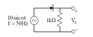
Q: The output V0 of the diode circuit shown in the figure is connected to an averaging DC voltmeter. The reading on the DC voltmeter in Volts, neglecting the
voltage drop across the diode, is ____________.
Q: The output V0 of the diode circuit shown in the figure is connected to an averaging DC voltmeter. The reading on the DC voltmeter in Volts, neglecting the
voltage drop across the diode, is ____________.
GATE-2017
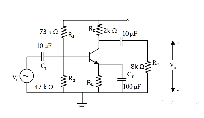
Q: For the DC analysis of the Common-Emitter amplifier shown, neglect the base current and assume that the emitter and collector current are equal. Given that VT = 25mV, VBE = 0.7V, and the BJT output r0 is practically infinite. Under these conditions the midband voltage gain magnitude, av = |v0/v1| V/V, is _____
GATE-2015
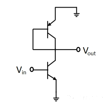
Q: In the ac equivalent circuit shown, the two BJTs are biased in active region and have identical parameters with β >> 1. The open circuit small signal voltage gain is approximately _______.
GATE-2013
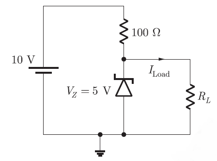
Q: In the circuit shown below, the knee current of the ideal Zener dioide is 10 mA . To maintain 5 V across RL, the minimum value of RL in Ω and the minimum power rating of the Zener diode in mW, respectively, are
- A: 125 and 125
- B: 125 and 250
- C: 250 and 125
- D: 250 and 250
GATE-2012
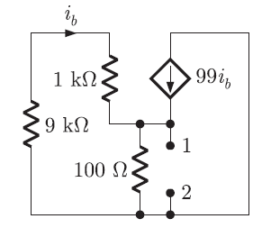
Q: The impedance looking into nodes 1 and 2 in the given circuit is
- A: 50Ω
- B: 100Ω
- C: 5kΩ
- D: 10.1kΩ
GATE-2011
Q: For a BJT, the common base current gain α = 0.98 and the collector base junction reverse bias saturation current ICO = 0.6 mA. This BJT is connected in the common emitter mode and operated in the active region with a base drive current IB = 20 mA. The collector current IC for this mode of operation is
- A: 0.98mA
- B: 0.99mA
- C: 1.0mA
- D: 1.01mA
GATE-2008
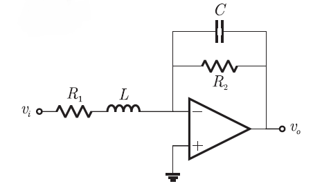
Q: The OPAMP circuit shown above represents a
- A: high pass filter
- B: low pass filter
- C: band pass filter
- D: band reject filter
GATE-2007
Q: In a transconductance amplifier, it is desirable to have
- A: a large input resistance and a large output resistance
- B: a large input resistance and a small output resistance
- C: a small input resistance and a large output resistance
- D: a small input resistance and a small output resistance
GATE-2006
Q: The input impedance (Zi) and the output impedance (Z0) of an ideal transconductance (voltage controlled current source) amplifier are
- A: Zi = 0,Z0 = 0
- B: Zi = 0,Z0 = ∞
- C: Zi = ∞,Z0 = 0
- D: Zi = ∞,Z0 = ∞
GATE-2005
Q: The effect of current shunt feedback in an amplifier is to
- A: increase the input resistance and decrease the output resistance
- B: increases both input and output resistance
- C: decrease both input and output resistance
- D: decrease the input resistance and increase the output resistance