QuestionPapersHub.com
GATE-2015
Q: Which one of the following processes is preferred to form the gate dielectric (SiO2) of MOSFET?
- A: Sputtering
- B: Molecular Beam Epitaxy
- C: Wet Oxidation
- D: (Dry Oxidation
GATE-2015
Q: If the base width in a bipolar junction transistor is doubled, which one of the following statements will be TRUE?
- A: Current gain will increase
- B: Unity gain frequency will increase
- C: Emitter base junction capacitance will increase
- D: Early voltage will increase
GATE-2014
Q: The current in an enhancement mode NMOS transistor biased in saturation mode was measured to be 1 mA at a drain to source voltage of 5 volts. When the drain – source voltage was increased to 6 volts, while keeping gate-source voltage same, the drain current increased to 1.02 mA. Assume that drain to source saturation voltages is much smaller than the applied drain source voltage. The channel length modulation parameter λ (in V-1) is __________
GATE-2013
Q: In a forward biased pn junction diode, the sequence of events that best describes the mechanism of current flow is
- A: injection, and subsequent diffusion and recombination of minority carriers
- B: injection, and subsequent drift and generation of minority carriers
- C: extraction, and subsequent diffusion and generation of minority carriers
- D: extraction, and subsequent drift and recombination of minority carriers
GATE-2013
Q: In a MOSFET operating in the saturation region, the channel length modulation effect causes
- A: an increase in the gate-source capacitance
- B: a decrease in the transconductance
- C: a decrease in the unity-gain cutoff frequency
- D: a decrease in the output resistance
GATE-2011
Q: The source of a silicon (ni=103 per cm3 ) n-channel MOS transistor has an area of 1 sq μm and a depth of 1 mm. If the dopant density in the source is 1019/cm3, the number of holes in the source region with the above volume is approximately
- A: 107
- B: 100
- C: 10
- D: 0
GATE-2010
Q: Thin gate oxide in a CMOS process in preferably grown using
- A: wet oxidation
- B: dry oxidation
- C: epitaxial oxidation
- D: ion implantation
GATE-2009
Q: In an n-type silicon crystal at room temperature, which of the following can have a concentration of 4 X 1019 cm-3?
- A: Silicon atoms
- B: Holes
- C: Dopant atoms
- D: Valence electrons
GATE-2008
Q: Which of the following is NOT associated with a p - n junction ?
- A: Junction Capacitance
- B: Charge Storage Capacitance
- C: Depletion Capacitance
- D: Channel Length Modulations
GATE-2008
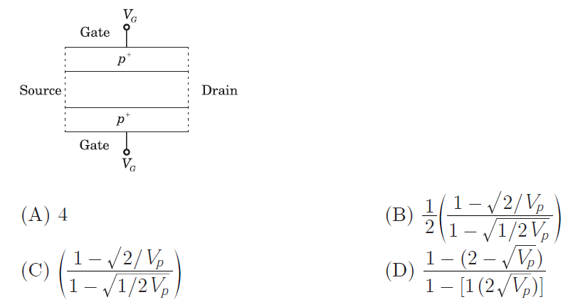
Q: The cross section of a JFET is shown in the following figure. Let Vc be -2 V and let Vp be the initial pinch -off voltage. If the width W is doubled (with other geometrical parameters and doping levels remaining the same), then the ratio between the mutual trans conductances of the initial and the modified JFET is