MUMBAI UNIVERSITY
Paper solution of EDC-1 Nov/Dec-2019
B. E. (Electronics & Telecommunication Engineering-CBCGS)-Sem-3
Subject (Subject Code): Electronic Devices & Circuits-1 (51202)
Date: 18/11/2019
Time: 3 Hrs.
Marks: 80
Instructions to the Students :
- Question no. 1 is compulsory.
- Solve any three questions from the remaining 5.
- Use of non-programmable scientific calculators is allowed.
- Assume suitable data wherever necessary & mention it clearly.
Q.1. Attempt any 4 (20).
a) Explain various types of Resistors.
b)Give the equation for the current in semiconductor diode. With the help of this equation explain in detail the V-I characteristics of a semiconductor diode.
c) Explain zener as a Voltage Regulator.
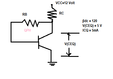
d) Find values of RB & RC:
e) Compare BJT CE Amplifier & JFET CS Amplifier.
f) Draw & explain high frequency model of BJT for CE configuration.
Q.2. (20)
Design a single stage CE Amplifier suitable for low frequencies of 10HZ to give voltage gain Av 70 & the output voltage of 4.5V; employing transistor type BC147A. Calculated the expexted Av & the maximum output voltage with negligible distortion that can be obtained from the designed circuit. Also, calculate the input resistance of the amplifier. Specify clearly the supply voltage Vcc for the designed circuit.
Q.3. (20)
a)A dc voltage of 350 volts with peak ripple voltagenot exceeding 5 Volts is required to supply a 500 Ω load. Determine the following if inductor filter & full wave rectifier is used:
- Inductance required
- Input voltage required
b) Explain & derive expression for ripple factor for capacitor filter with full wave rectifier.
Q.4. (20).
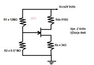
a) For the circuit shown below, determine IDQ & verify if the FET will operate in pinch off region:
b) State & explain Miller Theorem
Q.5. (20).
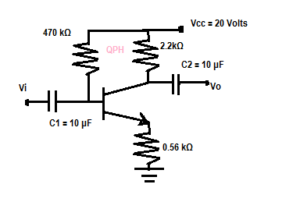
a) DetermineZi, Zo & Av for the circuit shown below:
b) Draw small signal hybrid parameter equivalent crcuit for CE amplifier & define the same. What are advantages of h-parameters?
Q.6. (20)
Write a short note on:
- hybrid parameter
- regions of opertion of FET
- stability factor of biasing circuits
- DC load line concept in BJT. Why Q point should be at the middle of the load line & fixed?
Paper End