Answer :
The timing diagram for write operation in minimum mode is shown in fig above:
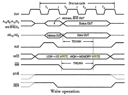
- When processor is ready to initiate the bus cycle, it applies a pulse to ALE during T1. Before the falling edge of ALE, the address, BHE, M/IO, DEN and DT/R must be stable i.e. DEN = high and DT/R = 0 for input or DT/R = 1 for output.
- At the trailing edge of ALE, ICs 74LS373 or 8282 latches the address.
- During T2 the address signals are disabled and S3-S7 ale available on AD16/S3-AD19/S6 and BHE/S7. Also DEN is lowered to enable transceiver.
- In case of input operation, RD is activated during T2 and AD° to AD15 go in high impedance preparing for input.
- If memory or I/O interface can perform the transfer immediately; there are no wait states and data is output on the bus during T3.
- After the data is accepted by the processor, RD is raised high at the beginning of T4. Upon detecting this transition during T.4, the memory or I/O device will disable its data signals. For an output operation, processor applies WR = 0 and then the data on the data bus during T2. In T4, WR is raised high and data signals are disabled.
- For either input or output operation, DEN is raised during 14 to disable the transceiver. Also M/I0 is set according to the next transfer at this time or during next T1 state. Thus length of bus cycle in 8086 is four clock cycle.
- If the bus is to be inactive after completion of bus cycle, then the gap between the successive cycles is filled by ideal state clock cycles.
- When the memory or I/O device is not able to respond quickly during transfer, wait states (Tw) are inserted between T3 and T4 by disabling the READY.